The Indium Phosphide Squeeze: The III-V Bottleneck Behind Every AI Optical Link...
Lumentum Undershipping Demand by 30%, 2.6x Surge in 800G+ Shipments by 2026, Three Substrate Makers Control the World's InP, Nvidia Locking EML Capacity Through 2027

For Indian businesses, you can check my writings at financepulse
Disclaimer: Before we begin, I am not a registered analyst. I’m just a student trying to study different businesses/sectors. Don’t take my word for it; try to study the businesses independently. I might have positions in the securities discussed. I am not an industry insider, so take my writings with a pinch of salt.
Broadcom’s Hock Tan said it on his last earnings call. Demand for optical components like lasers and pin diodes is “just going nuts.”
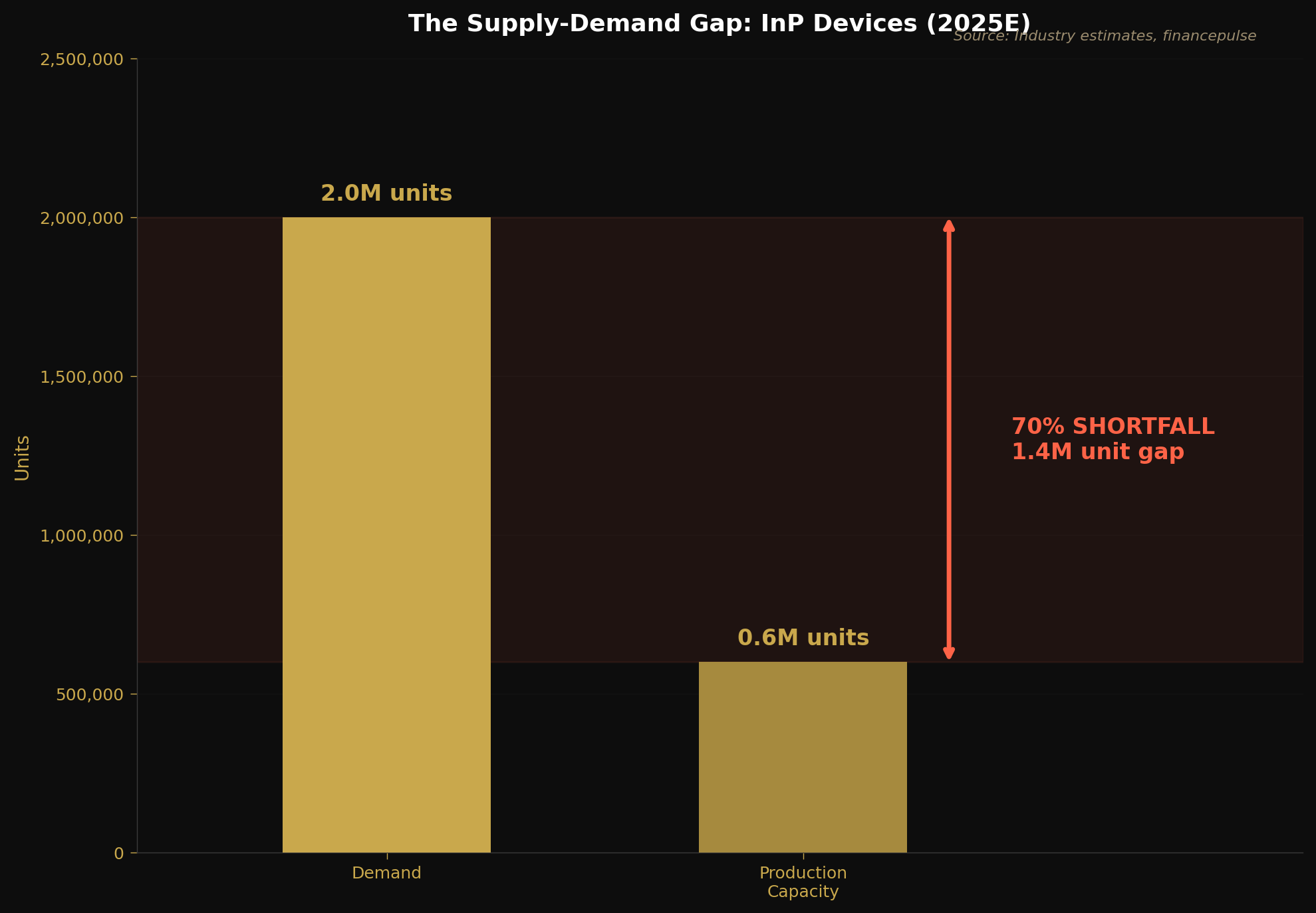
And right now, industry estimates suggest the world needs roughly 2 million InP devices per year. Production capacity? About 600,000. If those numbers are even directionally right - and we’ll scrutinize them later in this note - that is a severe supply-demand imbalance, and interesting investment setup for investors.
Lumentum’s CEO Michael Hurlston told analysts in February 2026 that his company is “undershipping customer demand by somewhere around 30%” - and that all EML capacity is spoken for through 2027 under long-term agreements. Coherent’s Jim Anderson said the same thing from the other side: “Our data center growth in Q1 was constrained by the supply of indium phosphide lasers.”
The silicon photonics narrative - the idea that silicon will replace InP - is the most misunderstood dynamic in the entire supply chain. I’ll explain why in detail later in this post, but the short version is this: silicon cannot generate light. Every silicon photonics platform - Intel’s, Broadcom’s, Cisco’s, Marvell’s - requires an InP-based laser to function. The shift toward silicon photonics and co-packaged optics doesn’t reduce InP demand. It changes the form factor while keeping InP at the center.
The market is starting to wake up at the device layer - Lumentum’s stock went from roughly $60 to $370 in a year, eight consecutive earnings beats, with Q3 FY2026 guidance implying 85% year-over-year growth. But i believe the upstream layers remain mispriced. The substrate layer has multi-year qualification moats and only three meaningful suppliers globally. The device layer is dominated by two companies - Coherent and Lumentum - whose combined InP laser capacity is fully booked for the next two years. The epitaxy layer is expanding but still constrained by MOCVD reactor lead times. And the raw material itself sits behind a Chinese export control regime that has already demonstrated its willingness to weaponize supply.
This is a supply chain where the “highest bidder wins” has become the norm for substrate allocation, where InP substrate prices have risen 3-5% with epitaxy prices following, where management teams at every layer are talking about “constraints” and “allocation” and “sold out” - and where the demand trajectory shows no sign of slowing. Worldwide shipments of 800G and higher optical transceivers are projected to jump from 24 million units in 2025 to nearly 63 million units in 2026. Each 800G transceiver uses four InP-based EML lasers. Each 1.6T transceiver uses eight. That is a doubling of InP content per module on top of a 2.6x increase in module shipments.
The Indium Phosphide Supply Chain
The InP wafer market itself is relatively small - approximately $198-211 million in 2025 - but it sits at the base of a datacom transceiver market heading toward $30 billion by 2026. Big-5 hyperscaler capex is projected at approximately $541 billion in 2026, growing 36% year-over-year, with optical transceivers representing 3-5% of total AI datacenter capex - a small share but mission-critical. Photonics and optical transceivers account for 58.9% of InP wafer consumption. Asia-Pacific commands 41.5% of the market.
WHY INP AND NOT SILICON
We need to address the most common pushback first: “Won’t silicon photonics replace InP?”
No. And the reason is physics.
Silicon is an indirect bandgap semiconductor. It cannot emit light efficiently. You can build waveguides in silicon, modulators in silicon, detectors in silicon. You cannot build a laser in silicon. Every silicon photonics platform on the planet - Intel’s, Broadcom’s, GlobalFoundries Fotonix, Marvell’s, Cisco’s - requires an InP-based laser source bonded, flip-chipped, or externally coupled to the silicon PIC.
InP has a direct bandgap at the exact wavelengths that fiber optics use (1310nm and 1550nm). Its electron mobility is nearly 10x that of silicon. InP modulators exceed 120 GHz bandwidth - silicon photonics hits a ceiling around 70 GHz. For the demanding requirements of 800G, 1.6T, and 3.2T optical links, InP is the only material that can simultaneously generate, modulate, amplify, and detect light on a single chip.
The irony is that the more silicon photonics wins, the more InP wins. They are complementary, not competitive. Silicon handles the integration. InP handles the photons. And silicon photonics is winning fast - SiPh transceiver market share rose from 10% in 2018 to 33% in 2024, and industry estimates project 50-60% share in 800G and 60-70% share in 1.6T segments by 2026. Every percentage point of SiPh share gain is another InP CW laser order. You can think of it like a hybrid car - silicon is the electric motor (efficient, scalable), InP is the engine (can’t be replaced for raw performance). And unlike hybrid cars, there is no pure-electric alternative on the horizon.
SUPPLY CHAIN MAPPING
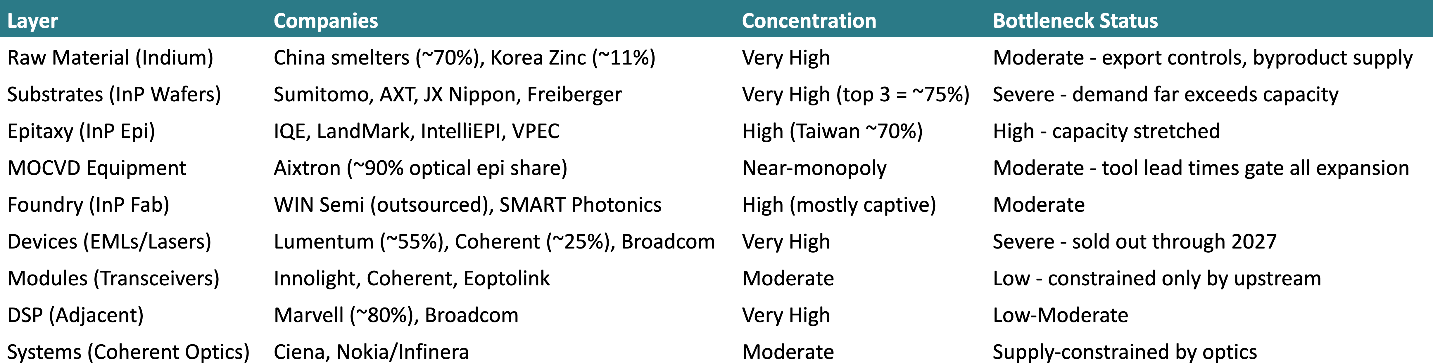
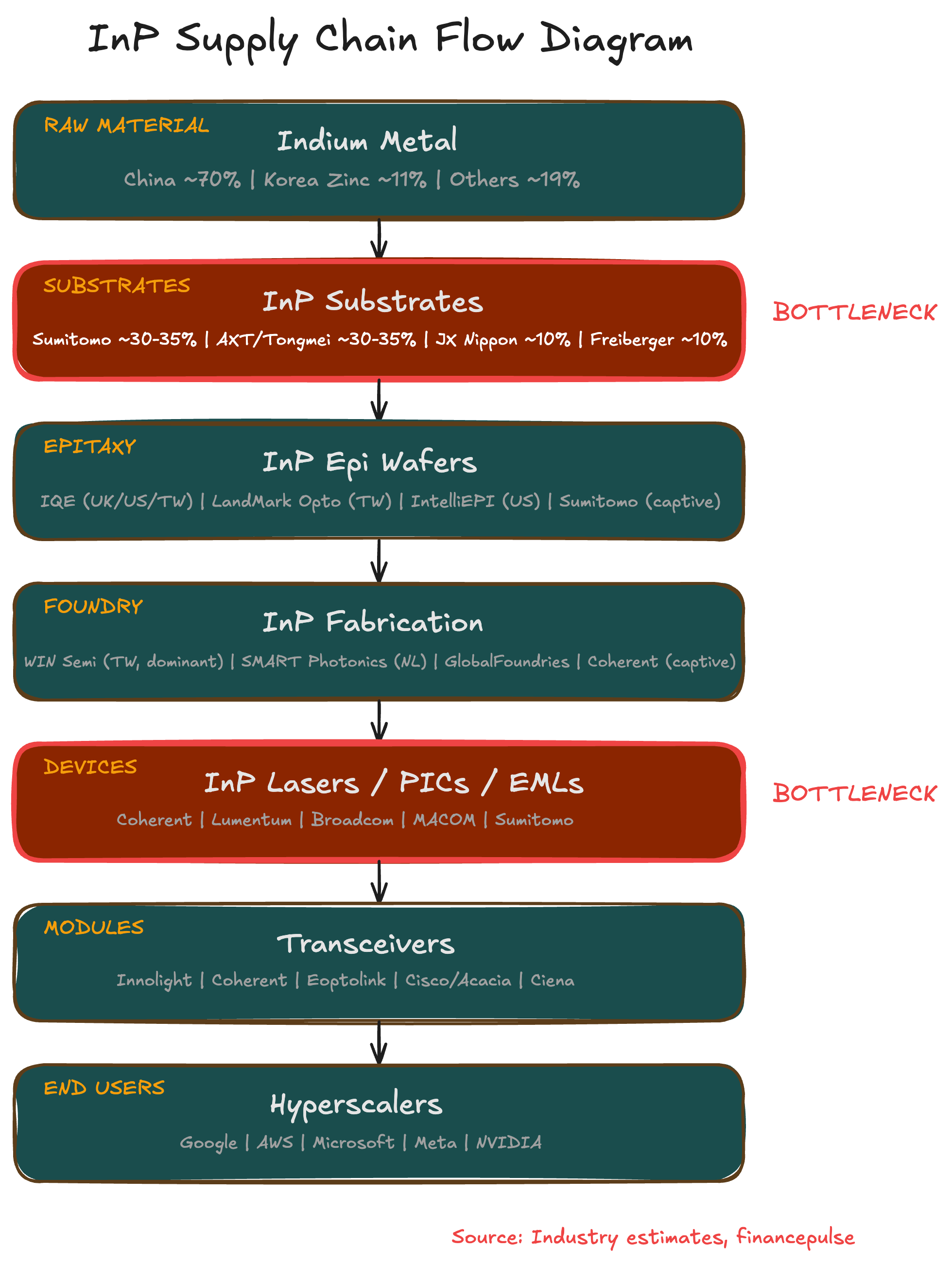
The InP supply chain has seven layers.
LAYER 1: INDIUM METAL - THE ZINC BYPRODUCT TRAP
Indium is never mined directly. It is recovered exclusively as a byproduct of zinc smelting, at a staggering ratio of 50,000 kg of zinc ore per 1 kg of indium extracted. Global refined indium production totaled about 1,080 metric tons in 2024. You cannot scale indium production independently of zinc mining - it is physically impossible.
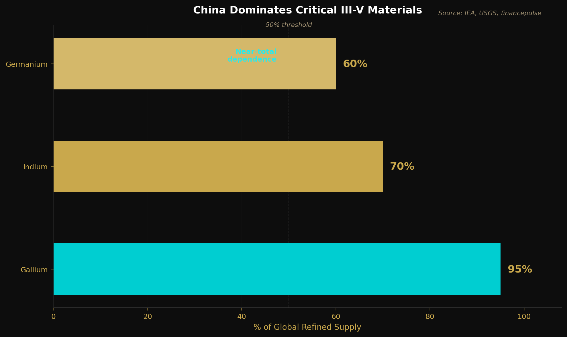
China produces approximately 70% of the world’s refined indium. On February 4, 2025 - minutes after Trump imposed additional tariffs on Chinese goods - Beijing announced export controls on indium and four other critical metals. This was not a ban, but a licensing requirement that effectively slows every shipment and creates regulatory chokepoints.
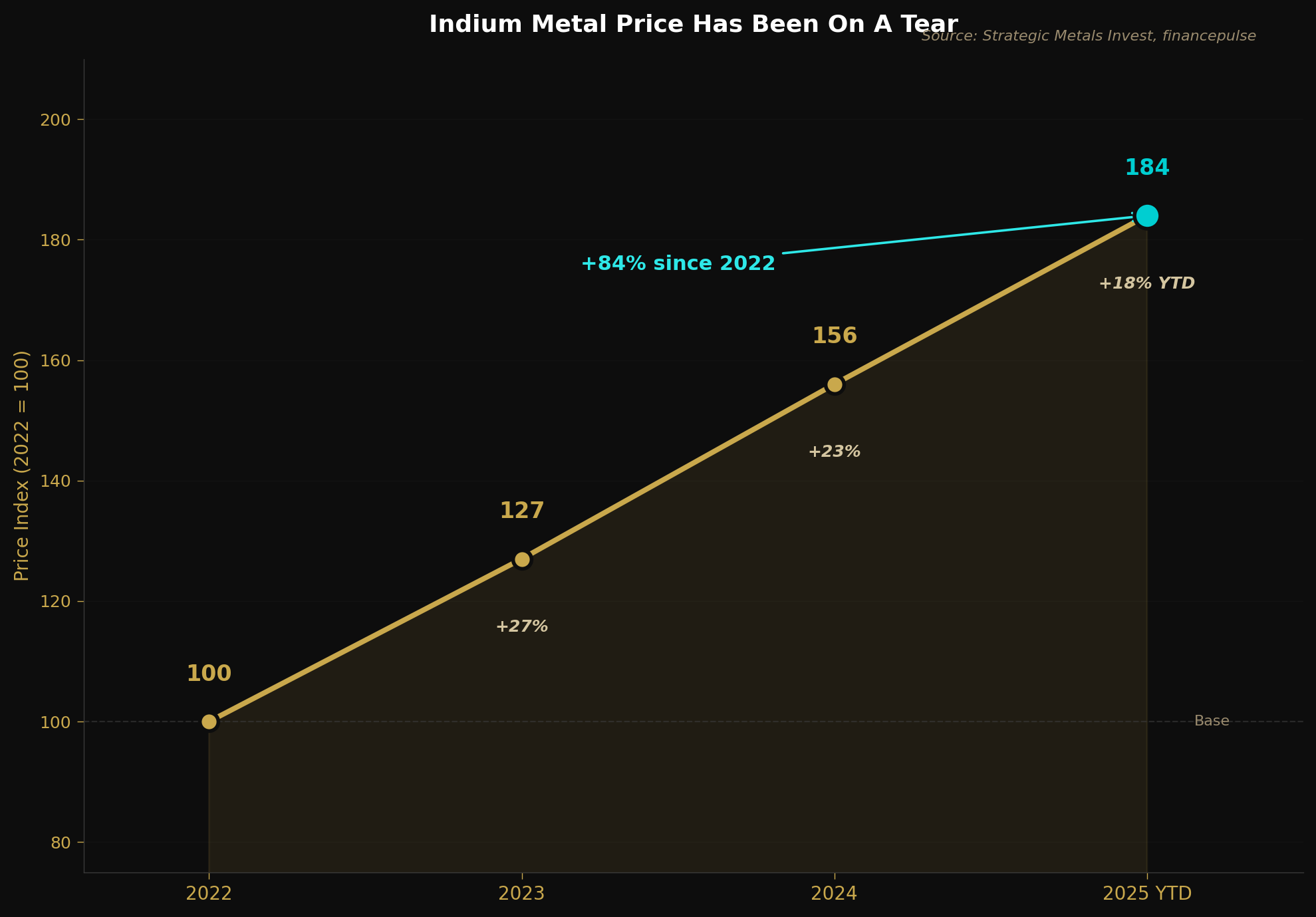
Indium prices have nearly doubled since January 2023, rising from roughly $445/kg to $867/kg by early 2026. The export controls amplified a trend already driven by surging AI-related demand. Korea Zinc, the world’s largest single refined indium producer at about 150 tons/year (~11% of global supply), has positioned itself as the critical non-Chinese source. But diversifying away from China will take years.
LAYER 2: INP SUBSTRATES - THE CHOKEPOINT THAT CONTROLS EVERYTHING
This is where the supply chain gets tight. Making high-quality InP crystal boules and slicing them into substrate wafers is an extraordinarily difficult process. InP has high decomposition pressure at its melting point, is prone to twinning defects, and is significantly more brittle than GaAs (the other major III-V compound semiconductor). Yields are under 30%. Qualification of new substrates by downstream device makers takes 12-18+ months.
companies controlling the world’s InP substrate supply:
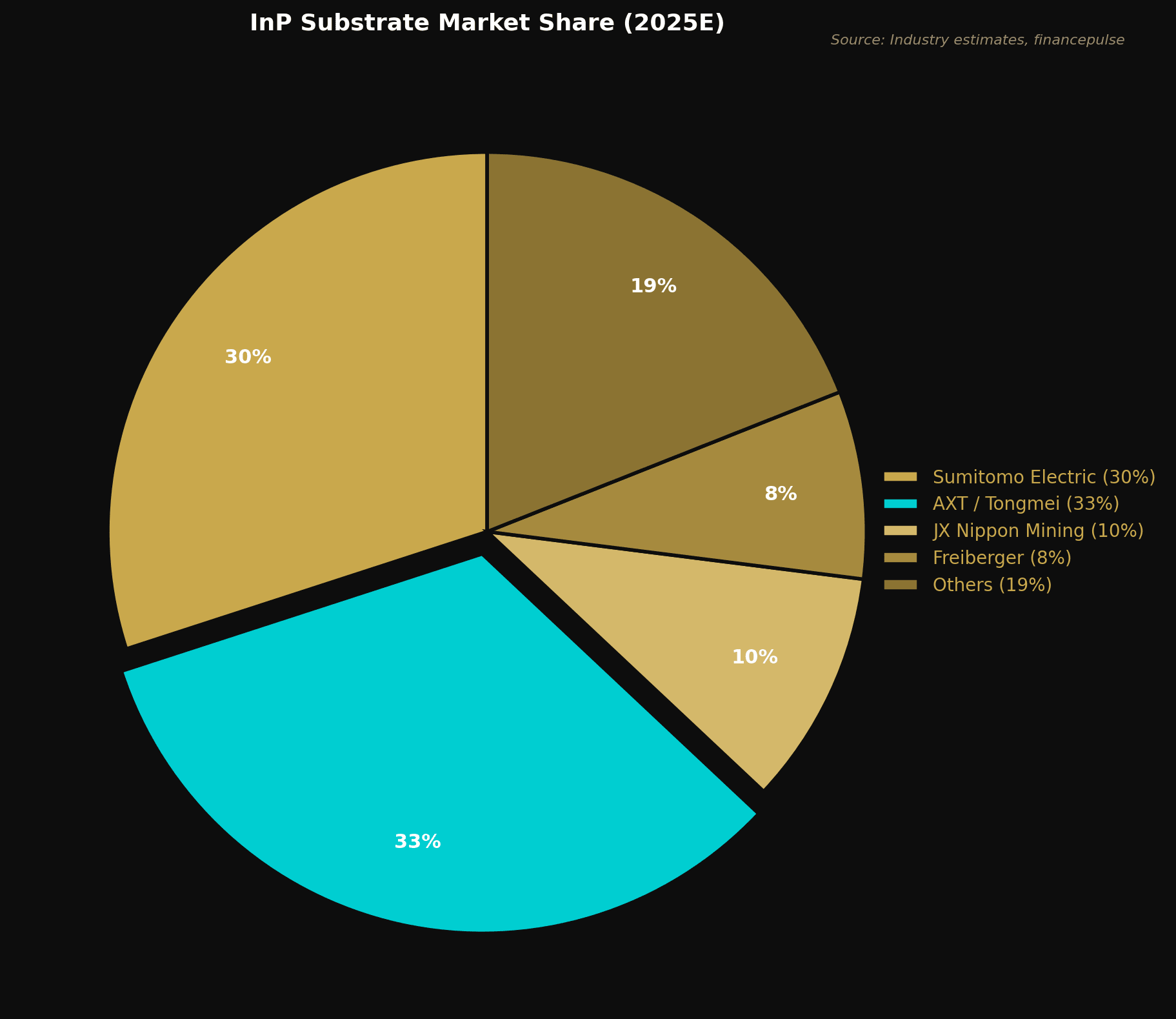
Sumitomo Electric Industries (5802 JP) holds roughly 30-35% share and uses the VB (Vertical Bridgman) crystal growth method. They are vertically integrated from substrates all the way to optical devices and CPO components. They have announced a 40% capacity expansion by 2026-2027, but management has indicated this could take “two and a half to three years.”
AXT Inc / Beijing Tongmei (AXTI) holds roughly 30-35% share using the VGF (Vertical Gradient Freeze) method, which offers cost advantages. AXT is the only publicly listed pure-play InP substrate company. Its Q3 2025 was remarkable - InP revenue surged 250% sequentially to $13.1 million, backlog more than doubled to a record $49 million. CEO Morris Young claims “40% of the indium phosphide supply chain” and says AXT wafers produce higher device yields for customers.
But AXT has a problem. Its manufacturing is in Beijing through subsidiary Tongmei, and China’s February 2025 export controls require permits for every InP shipment leaving the country. Permits take about 60 business days to process. The first half of 2025 saw zero permits issued. Permits resumed in Q3, but Q4 revenue was cut to $22.5-23.5M after fewer permits than expected.
JX Nippon Mining & Metals holds roughly 10% share from its Isohara plant in Ibaraki, Japan. JX has been aggressively expanding - investing Y3.3 billion for a 50% capacity increase versus 2025 levels, with management promising at least one more expansion announcement. They have positioned InP substrates as core to their “Long-Term Vision 2040.”
Freiberger Compound Materials (Germany) holds about 8% share, producing 2-inch to 4-inch InP substrates and providing important European supply chain diversification.
Chinese domestic capacity is emerging but remains early-stage for tier-1 applications. Huawei-backed Yunnan Xinyaoalready produces 150,000 2-4 inch InP wafers annually. Sanan Optoelectronics (600703 CH), China’s largest compound semiconductor foundry, is expanding 6-inch InP capability. CETC (China Electronics Technology Corporation) has state-backed InP wafer and device programs, and Accelink Technologies (002281 CH) in Wuhan is developing InP laser capability. Chinese EML localization remains at only about 4% for 25G+ speeds, and reliability qualification at Western laser manufacturers will take years. But the trajectory of Chinese semiconductor localization in other areas - mature-node logic, NAND, DRAM - suggests these players should not be dismissed.
According to industry estimates global demand for InP devices at 2 million pieces in 2025 versus production capacity of only 600,000 pieces. Orders at leading suppliers are fully booked until 2026. IntelliEPI’s chairman said “even capacity increases of 20% to 30% by substrate suppliers have failed to keep pace” and “the gap between supply and demand is likely to widen.”
LAYER 3: EPITAXIAL WAFERS - TAIWAN’S SWEET SPOT
Epitaxy is where precisely engineered crystalline layers are grown onto InP substrates using MOCVD or MBE reactors. These are the layers that actually emit, detect, or modulate light. Taiwanese companies dominate this layer with approximately 70% of global InP epitaxy market share.
IQE PLC (IQE LN) is the only pure-play epi-wafer producer with scale across all major platforms (MOCVD and MBE) and the broadest material portfolio (GaAs, InP, GaSb, GaN). FY2025 revenue was approximately GBP 97 million, with photonics revenue of GBP 26.6 million in H1, driven by “strong performance in InP data communications for AI markets.” IQE launched a 6-inch foundry platform for silicon photonics and secured multiple design wins for AI data center applications. But the company is under strategic review - the board is negotiating potential sale offers, including for its Taiwan operations. If IQE gets acquired, it would further concentrate the InP epitaxy supply chain.
LandMark Optoelectronics (3081 TT) is Taiwan’s InP epi specialist, making DFB epi-wafers, EML epi-wafers, APD epi-wafers, and PIN PD epi-wafers. Revenue grew 52% year-over-year on a trailing twelve-month basis as of September 2025, with Q3 2025 revenue of TWD 552.8 million up 71% quarter-over-quarter. The company operates 27 MOCVD reactors and is adding more to sustain what management describes as a threefold SiPh shipment growth trajectory. LandMark expects strong 800G demand through 2026 and is forecasting faster sequential revenue growth in Q1 2026 than in Q4 2025.
IntelliEPI (iET) operates from both Taiwan and Texas, focusing on InP epitaxy outsourcing. It was the first to develop “production ready” 4x4 inch InP capabilities and won a $4.12 million Texas Semiconductor Innovation Fund grant. IntelliEPI is a critical overflow partner as laser makers prioritize their own laser epitaxy and outsource photodiode epitaxy.
As EML and CW laser demand outstrips internal capacity at device makers, more epitaxy work is being outsourced to specialists like IntelliEPI and VPEC (Visual Photonics Epitaxy, 2455 TT). VPEC recently entered Furukawa’s 800G transmitter supply chain and expects 50% year-over-year growth in optical revenue. This outsourcing dynamic is a signal of how tight the epitaxy layer has become.
There is a bottleneck behind the bottleneck that deserves attention. Every InP epitaxy expansion - whether at LandMark, VPEC, Coherent, or Nokia’s newly acquired Infinera operation - requires MOCVD (Metal-Organic Chemical Vapor Deposition) reactors to grow the crystal layers. Aixtron (AIXA GR) holds approximately 90% market share in optical component epitaxy MOCVD tools. Its G10-AsP platform, specifically designed for arsenide/phosphide applications, is the workhorse behind virtually every InP capacity expansion underway. Nokia, SMART Photonics, Coherent, Furukawa Electric, and Lumcore have all placed orders for G10-AsP systems. LandMark operates 27 MOCVD reactors and is adding more. If MOCVD tool delivery itself becomes the gating factor - and lead times on these systems run months - then Aixtron’s production schedule effectively sets the ceiling on how fast the entire InP supply chain can expand.
LAYER 4: FOUNDRY / FABRICATION
WIN Semiconductors (3105 TT) is the world’s largest pure-play compound semiconductor foundry with approximately 65% market share and annual capacity exceeding 500,000 wafers. WIN offers InP foundry services for optical devices on 2-inch to 4-inch substrates. WIN is relevant as a potential InP capacity source if demand outstrips what Coherent and Lumentum can produce internally.
SMART Photonics (Netherlands, private) is Europe’s leading independent InP PIC foundry. Their InP modulators exceed 120 GHz bandwidth versus about 70 GHz for leading silicon photonics. SMART recently transitioned from 3-inch to 4-inch production and secured approximately EUR 100 million in funding with EU Chips Act support, with a target of 50,000 wafer starts/year.
GlobalFoundries (GFS) operates the GF Fotonix platform - a silicon photonics platform, not a native InP foundry. But GF is increasingly important for heterogeneous InP integration. Its acquisition of Advanced Micro Foundry (AMF) in Singapore in November 2025 bolstered InP-on-silicon capabilities. Design wins include Broadcom, Cisco, Marvell, NVIDIA, and startups like Ayar Labs and Lightmatter.
Most InP device fabrication remains captive - Coherent, Lumentum, Broadcom, and Sumitomo all fabricate their own InP devices. This is unlike silicon where foundry outsourcing is the norm. The reason is that InP device fabrication involves proprietary epitaxial recipes and processing knowledge that companies guard fiercely.
LAYER 5: DEVICE / COMPONENT MAKERS - THE EML SHORTAGE THAT CHANGES EVERYTHING
This is where the supply chain crisis is most acute. Electro-absorption Modulated Lasers (EMLs) combine laser generation and signal modulation on a single InP chip. They are the critical component inside every 800G and 1.6T transceiver. Each 800G module requires 4-8 InP laser chips. A 1.6T module uses 8 EML lasers at 200G per lane versus 4 at 100G per lane for 800G - doubling the InP laser chip count per transceiver, with higher-performance devices that require larger die sizes.
TrendForce reports that NVIDIA has secured capacity at key EML suppliers, pushing lead times beyond 2027 and triggering a worldwide shortage. Lumentum’s CEO has started “culling customers” to focus supply on strategic accounts. Coherent’s data center growth was “constrained by the supply of indium phosphide lasers” - and they make their own lasers.
The alternative to EML-based transceivers is CW (continuous wave) lasers combined with silicon photonics. Instead of modulating light on the InP chip, you use a simple InP CW laser source and modulate on the silicon PIC. But CW production faces its own constraints: long equipment lead times, labor-intensive testing, and outsourcing dependencies. The CW ecosystem is approaching its own capacity crunch.
This is the punchline: even the alternative to InP EMLs still requires InP for the laser source. You cannot escape indium phosphide in high-speed optical communication.
The optical communication chip market - encompassing EMLs, CW lasers, VCSELs, and photodetectors - is projected to grow from approximately $3.5 billion in 2024 to over $11 billion by 2030. Combined advanced optical chip capacity (CW + EML + VCSEL) from major global suppliers is expected to increase by more than 80% year-over-year in 2026. Even with that expansion, industry estimates suggest capacity will still lag demand by 5-15%. The supply chain is sprinting to catch up and still falling behind.
LAYER 6: MODULE / TRANSCEIVER MAKERS
Chinese manufacturers led by Zhongji Innolight (300308 CH) and Eoptolink (300502 CH) have captured approximately 60% of NVIDIA’s 800G transceiver requirements. Innolight reported revenue of RMB 23.86 billion in 2024 (+123% YoY). But these module makers are dependent on upstream InP laser supply from Lumentum, Coherent, and others.
Coherent is unique in competing at both the component and module levels - it makes its own InP lasers and assembles them into transceivers. At OFC 2025, Coherent was the only company to demonstrate three different 1.6T transceiver architectures: silicon photonics, EML, and VCSEL.
Ciena (CIEN) leads coherent optical systems with its WaveLogic 6 Extreme - the industry’s first 1.6 Tbps per wavelength solution using a 3nm ASIC. CEO Gary Smith called 2025 “a seminal year” and management said they are “essentially sold out” with supply constraints expected through 2027.
Marvell (MRVL) dominates optical DSPs with approximately 80% market share in PAM4, the modulation format inside every high-speed transceiver. Every transceiver that uses an InP laser also uses a Marvell DSP.
LAYER 7: END USERS - THE HYPERSCALER PULL
The hyperscalers - Google, Amazon, Microsoft, Meta, and NVIDIA - are the ultimate demand drivers. Each new AI GPU cluster requires exponentially more optical I/O.
NVIDIA has taken the unprecedented step of directly locking in EML laser capacity with suppliers, with lead times extending beyond 2027.
THE CPO TRANSITION: MORE INP, NOT LESS
Co-packaged optics (CPO) integrates optical engines directly onto the switch package, replacing traditional pluggable transceiver modules. The market narrative suggests CPO could reduce InP demand. I think the opposite is true.
Broadcom’s Tomahawk 6 Davisson - the industry’s first 102.4 Tbps CPO switch - is now shipping. Each CPO switch incorporates up to 16 photonic integrated circuits, each requiring InP laser sources. NVIDIA’s Quantum-X CPO package delivers 28.8 Tbps of bandwidth. At these densities, far more InP laser die are needed per switch than in traditional pluggable architectures.
The BOM breakdown of Nvidia’s Quantum X800 CPO switch provides further confirmation. At an estimated $80-90K per switch, the largest cost line is 72 optical engines at $36,000 (41% of BOM). But the InP-specific content is concentrated in the external laser source modules (18 units at $18,000, or 21% of BOM) and the CW lasers themselves (18 units at $4,320, or 5% of BOM). Combined, InP-based components represent approximately 26% of the CPO switch BOM. Compare that to a pluggable architecture where the InP laser content per port is a fraction of the module cost. CPO does not reduce InP intensity, it concentrates it at higher power levels and higher dollar content per system.
The CPO market is projected to grow from $46 million in 2024 to $8.1 billion by 2030 at a 137% CAGR. Lumentum has secured multiple multi-$100 million purchase orders for ultra-high power InP lasers for CPO applications. The 400mW power level these CPO lasers require is described as a barrier that “not many people can do.”
THE CAPACITY EXPANSION RACE
Everyone is expanding. But InP capacity takes years to build, and demand is growing faster than capacity can come online.
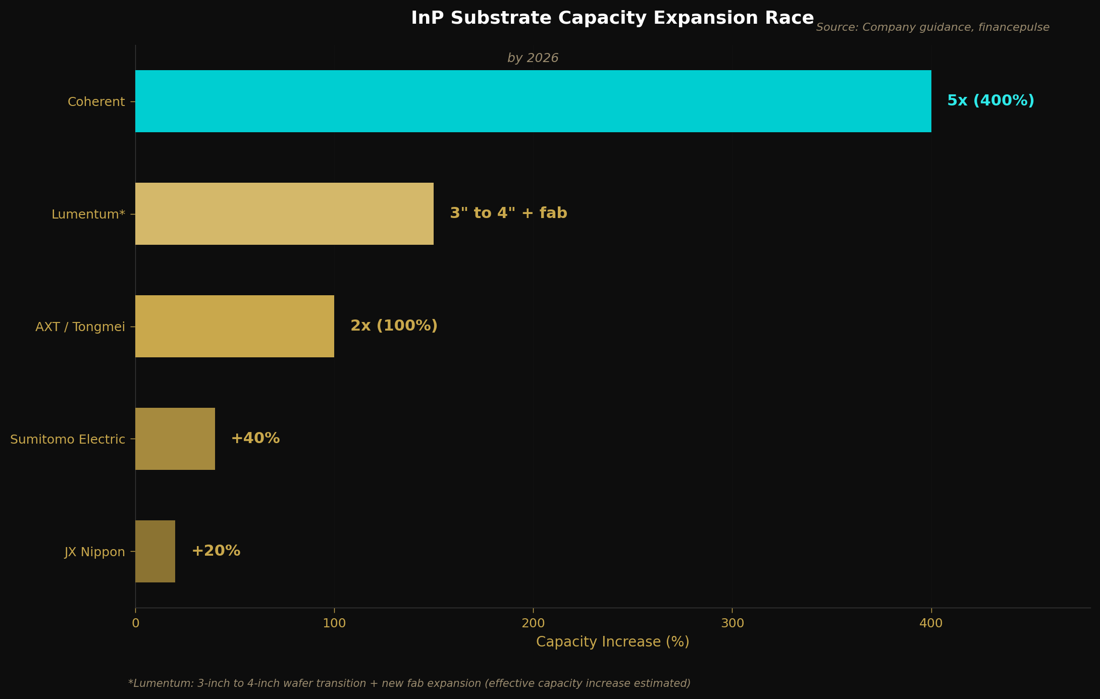
AXT plans to more than double InP capacity by H2 2026, leveraging repurposed GaAs crystal growth facilities for faster, cheaper expansion. But export permit uncertainty from China adds a wild card.
Sumitomo Electric is expanding capacity by 40% but management acknowledges a 2.5-3 year timeline.
JX Nippon has committed Y3.3 billion for 50% capacity expansion, operational by end of FY2027.
Coherent is the most aggressive, targeting 5x InP production capacity by 2026 through its 6-inch wafer transition across two sites (Sherman, Texas and Jarfalla, Sweden). Initial 6-inch yields already exceed mature 3-inch lines. CEO Jim Anderson: “A six-inch wafer, compared to a three-inch wafer, will produce more than four times as many chips at less than half the cost.” (I don’t buy it though)
Lumentum is investing heavily in its San Jose InP wafer fab, transitioning EML production from 3-inch to 4-inch wafers. The company added approximately 40% capacity in recent quarters and has line of sight to additional capacity in H2 2026. But even after adding 20% capacity, the demand gap has widened. At OFC 2025, Lumentum demonstrated a 448G EML operating at 448 Gbps using 224 GBaud PAM4 - the bleeding edge of InP modulator performance and a preview of what the 3.2T transceiver generation will require.
SUPPLY CHAIN BASKET
I identified 16 publicly traded companies across the InP supply chain, grouped by their role in the photon highway from mine to hyperscaler. Every company here touches indium phosphide in some meaningful way - some make the raw wafers, some grow the crystal layers, some turn those layers into lasers, some package lasers into modules, and some build the silicon platforms that need InP light sources to function.
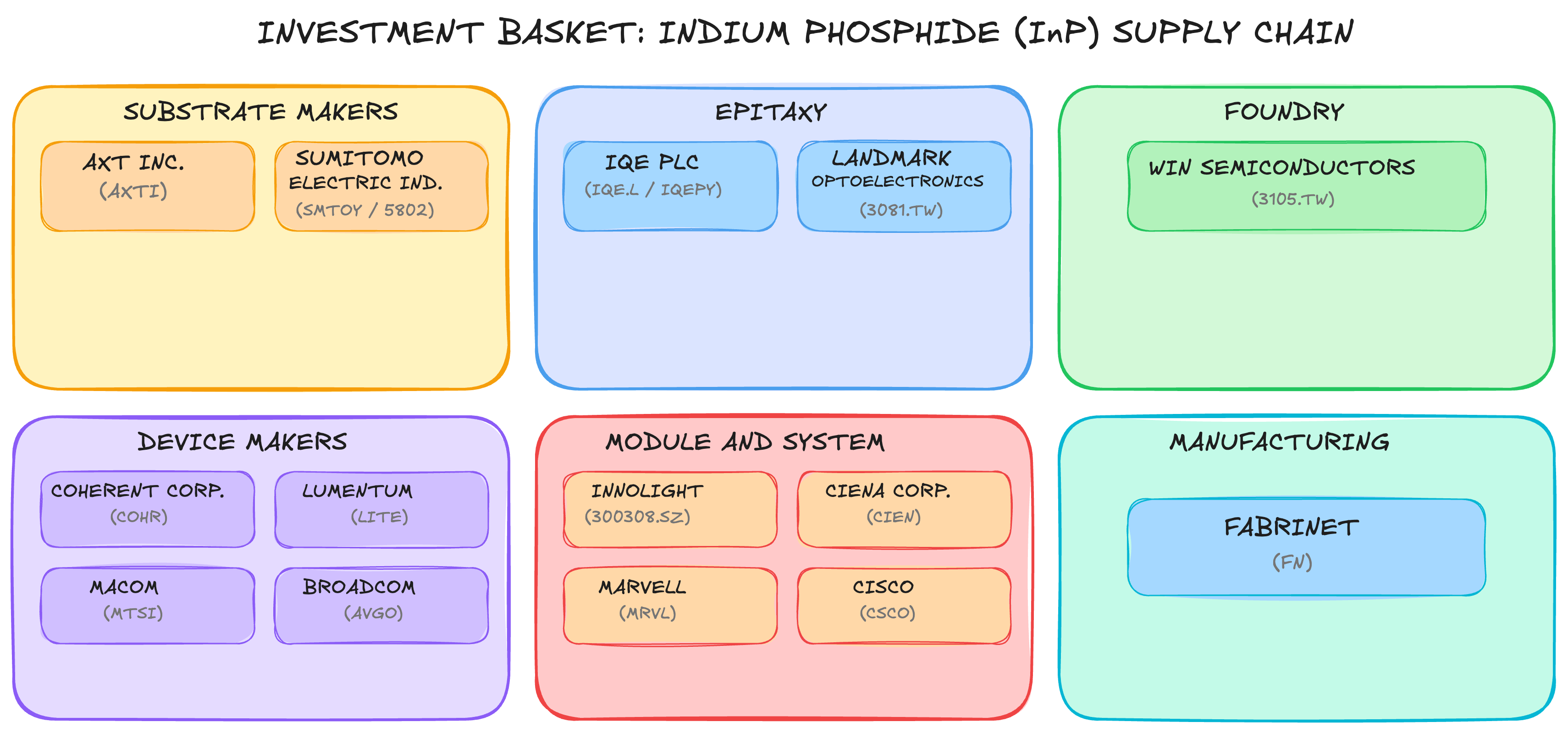
UPSTREAM SUBSTRATE MAKERS
These are the companies that grow InP crystals and slice them into wafers. This is where the supply chain begins after raw indium metal, and it is the tightest bottleneck in the entire chain.
AXT Inc (AXTI) - The Pure-Play Substrate Bet
AXT is the only publicly listed company whose primary identity is InP substrates. Through its Beijing subsidiary Tongmei, AXT holds roughly 30-35% of the global InP substrate market - some estimates put it as high as 40%. CEO Morris Young claims AXT wafers produce “better die yield” for customers’ lasers and detectors, which matters enormously when every device is sold out.
The company uses the VGF (Vertical Gradient Freeze) crystal growth method, which offers cost advantages over the VB method used by Sumitomo. AXT has also achieved mass production of 6-inch InP substrates, putting it ahead of most competitors on the wafer size curve.
Q3 2025 revenue hit $28 million, up 56% sequentially, with InP revenue surging 250% from $3.6 million to $13.1 million. The InP backlog more than doubled to a record $49 million. AXT raised $100 million in a December 2025 equity offering specifically to fund InP capacity expansion, targeting more than double current capacity by H2 2026. The company can repurpose an existing GaAs crystal growth building, enabling faster, cheaper expansion than competitors building from scratch.
But AXT’s China problem is real. Manufacturing happens in Beijing, and China’s February 2025 InP export controls require permits for every overseas shipment. Permits take approximately 60 business days. H1 2025 saw zero permits. They resumed in Q3 but slowed again in Q4, forcing a revenue guidance cut to $22.5-23.5 million. Morris Young acknowledges: “The receipt of export permits remains the single most significant gating factor for our growth.”
The bull case is that AXT is the purest way to play the InP substrate shortage - a company that is demonstrably gaining share, has pricing power it has never had, and is doubling capacity into multi-year demand. The bear case is that its manufacturing sits behind a Chinese government permit gate it cannot control.
Sumitomo Electric Industries (5802 JP) - The Vertical Giant
Sumitomo Electric is the quiet powerhouse of the InP supply chain. With approximately 30-35% substrate market share and vertical integration spanning from crystal growth through optical devices to co-packaged optics, Sumitomo touches nearly every layer of the chain. You can think of them as the Samsung of InP - they make everything internally. (I like them more like AXTI)
Sumitomo uses the VB method for InP crystal growth, producing 4-inch Fe-doped semi-insulating substrates with mature technology and stable yields. They have announced a 40% capacity expansion by 2026-2027, but management has indicated this could take “two and a half to three years” - slower than AXT’s repurposing approach.
What makes Sumitomo important is not just substrates. They manufacture InP laser diodes for fiber optic networks, produce photonic components, and at ECTC 2025 presented an innovative CPO integration platform combining glass substrates with 3D-printed VCBELs. They hold approximately 10% of the EML laser market.
EPITAXY SPECIALISTS
These companies grow the precise crystalline layers on InP substrates that actually function as lasers, detectors, and modulators. They sit between substrate makers and device fabricators.
IQE PLC (IQE LN) - The Global Epi House Under Strategic Review
IQE is unique in the compound semiconductor world. It is the only pure-play epitaxial wafer producer with scale across all major platforms - MOCVD and MBE - combined with the broadest material portfolio in the industry: GaAs, InP, GaSb, and GaN. Manufacturing spans the UK, USA, and Taiwan.
The InP story within IQE is strong. H1 2025 photonics revenue was GBP 26.6 million, with “strong performance in InP data communications for AI markets.” The company secured multiple customer design wins for laser and detector products enabling next-generation AI data center infrastructure. IQE also launched a 6-inch foundry platform for silicon photonics applications.
But the overall business is complicated. FY2025 revenue was approximately GBP 97 million, dragged down by wireless weakness. The board has expanded its strategic review to include a potential sale of the entire group, including separate bids for Taiwan operations. What makes IQE strategically important is concentration risk. If IQE gets acquired and its InP epitaxy capacity gets consolidated under a larger player, the independent epi supply chain narrows further.
LandMark Optoelectronics (3081 TT) - Taiwan’s InP Epi Specialist
LandMark is the purer InP epitaxy play. Based in Taiwan, the company specializes in InP and GaAs epitaxial wafers for optical communication. Trailing twelve-month revenue reached approximately TWD 1.85 billion as of September 2025, up 52% year-over-year. Q3 2025 revenue was TWD 552.8 million, up 71% quarter-over-quarter.
LandMark has been “successively expanding epitaxy capacity” with output projected to continue rising. Its silicon photonics revenue contribution moved from 42% in 2024 to 76% in 2025 - meaning the growth in SiPh is directly flowing through as InP epitaxy orders.
FOUNDRY / FABRICATION
WIN Semiconductors (3105 TT) - The Compound Semi Foundry
WIN Semiconductors is the TSMC of compound semiconductors - the world’s largest pure-play III-V foundry with approximately 65% market share and annual capacity exceeding 500,000 wafers. WIN is primarily known for GaAs foundry services serving RF and mobile markets, but its InP foundry capability is increasingly important.
The reason WIN matters for the InP thesis is optionality. If the EML and CW laser shortage drives device makers to outsource more InP fabrication, WIN is the most logical destination - it has the compound semiconductor fab infrastructure, the process expertise, and the capacity headroom (Q2 2025 utilization was only 45%).
DEVICE / LASER MAKERS
These companies turn InP substrates and epitaxial layers into the laser chips, photodetectors, and photonic integrated circuits that go inside transceivers. This is where the most acute shortage exists today.
Coherent Corp (COHR) - The Most Vertically Integrated Player in Photonics
Coherent (formerly II-VI, which acquired Finisar) is the only company in the world that manufactures its own InP substrates, grows its own epitaxy, fabricates its own laser devices, and assembles its own transceivers.
Coherent launched the world’s first 6-inch InP production line at its Sherman, Texas facility in September 2025, with a second line ramping in Jarfalla, Initial 6-inch yields already exceed mature 3-inch lines. The company is in production on three device types on 6-inch InP: EMLs, CW lasers, and photodiodes.
I think this claim warrants some skepticism. Moving to a larger wafer format in compound semiconductors typically involves a multi-year yield learning curve, and “higher yields on day one” is unusual. The comparison may benefit from newer equipment and cleaner facilities on the 6-inch line versus aging 3-inch tools.
Coherent recently received a $14 million Texas Semiconductor Innovation Fund grant to accelerate InP production, representing over $154 million in total capital investment. The company plans to roughly double InP production capacity over the next year and is targeting 5x current capacity by 2026.
Yet even Coherent is supply-constrained. F2Q26 results beat expectations - revenue of $1,686 million versus consensus of $1,641 million, with gross margins at 39% - and F3Q26 guidance of $1,700-1,840 million. But data center revenue growth remains “constrained by the supply of indium phosphide lasers.” The book-to-bill ratio for data center products exceeded 4x exiting F2Q26 - including transceivers, OCS, and CPO. Coherent has already met 80% of its wafer start target to double InP capacity internally and is also sourcing incremental capacity from external InP suppliers including Lumentum. The company is expanding manufacturing in Malaysia and Vietnam to support the order pipeline.
Lumentum Holdings (LITE) - The EML Laser Leader
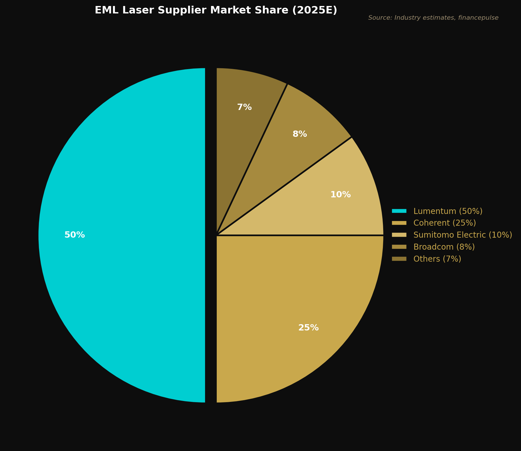
Lumentum is the single most important company in the InP supply chain. The company holds approximately 50-60% of the global EML market - the laser chips that go inside every 800G and 1.6T transceiver. Capacity is sold out through 2026 and largely booked through 2027 under long-term agreements.
Lumentum is the sole source for NVIDIA’s CPO laser supply, providing ultra-high power 1310nm DFB lasers engineered for co-packaged optics. The 400mW power level is described as a barrier “not many people can do.” Lumentum has secured multiple multi-$100 million purchase orders for CPO lasers, with shipments expected to begin in 2027.
The InP wafer fab transition is underway, moving EML production from 3-inch to 4-inch wafers at its San Jose facility, with expansion across Sagamihara and Takao (Japan) and Caswell (UK) fabs. The 200G EML ramp is particularly important for 1.6T transceivers: 200G devices represent about 5% of unit volume but 10% of data center laser chip revenue due to higher ASPs. That mix is expected to reach 25% by end of calendar 2026.
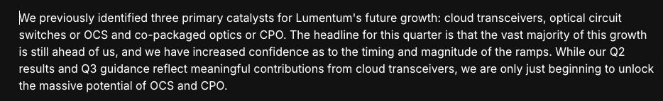
Lumentum’s OCS (optical circuit switching) business has emerged as a new growth vector pretty quickly. OCS backlog exceeded $400 million as of February 2026 - up from a prior $100 million target that management set barely a year ago. The quarterly OCS run rate already exceeds $100 million. Lumentum’s MEMS-based OCS technology competes with Coherent’s liquid crystal approach for hyperscaler switching.
MACOM Technology Solutions (MTSI) - The InP Photodetector Pivot
MACOM was traditionally seen as an RF and defense company. That perception is changing. CEO Stephen Daly described a “breakthrough” in Q4 FY2025: “We believe we have had a breakthrough where our cloud customers and their supply chain recognize the strategic value of MACOM’s proprietary indium phosphide technology and high-volume manufacturing capabilities.”
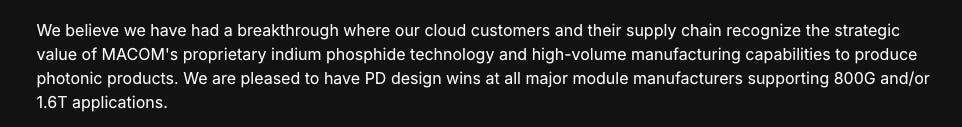
MACOM’s InP edge comes from its proprietary Etched Facet Technology (EFT), acquired through the BinOptics purchase for $230 million in 2014. The company’s 200G photodetector is described as having “industry-leading sensitivity and dark current performance.” Design wins are at “all major module manufacturers” for 800G and 1.6T applications. Data center revenue surged 48% in FY2025 to $293 million. Book-to-bill hit 1.3:1 - the highest since Q3 2021.
MACOM’s Ann Arbor, Michigan InP fab is approaching maximum capacity, and production is being transferred to its larger Massachusetts facility. The collaboration with GlobalFoundries on mass-produced L-PICs (laser-PICs) using GF’s 300mm silicon fabs is worth mentioning - MACOM’s EFT lasers can be aligned and attached directly to silicon photonics die, potentially positioning MACOM as a key bridge between InP and silicon photonics worlds.
MODULE / SYSTEM LAYER
GlobalFoundries (GFS) - Silicon Photonics With InP Integration
GlobalFoundries is not an InP company. Its GF Fotonix platform is a 300mm silicon photonics foundry service. But every silicon photonics transceiver that GF manufactures needs an InP CW laser attached to it, making GF a demand driver for InP rather than a substitute.
Silicon photonics revenue is on track to exceed $200 million in 2025, nearly doubling year-over-year. GF won three new optical networking designs in Q3 2025 worth $150 million+ in projected lifetime revenue. Management envisions silicon photonics becoming a $1 billion+ run-rate business before end of decade. As GF’s silicon photonics revenue doubles, InP CW laser demand grows proportionally.
RISKS TO THIS THESIS
Capacity catches up faster than expected. AXT is doubling capacity through 2026. Sumitomo is doubling over 2.5-3 years. JX Nippon announced a 50% capacity increase. Coherent’s 6-inch transition enables 4x more devices per wafer. If all expansions hit simultaneously and AI capex moderates, we could see substrate oversupply by 2027-28.
Heterogeneous integration reduces bulk substrate demand. InP-on-Si heterogeneous integration bonds InP die onto silicon wafers rather than using standalone InP substrates. Over time, this could reduce total InP substrate consumption even while InP material remains essential. Companies like Aeluma and OpenLight are pursuing this path. More concretely, X-FAB, SMART Photonics, and Epiphany Design launched an InP-on-Si heterogeneous photonics platform with commercial rollout targeted for 2027 - this could unlock InP PICs on silicon wafers at scale.
Chinese InP capacity reaches quality parity. Huawei-backed Yunnan Xinyao already produces 150,000 2-4 inch InP wafers annually. Sanan Optoelectronics is expanding 6-inch InP capability. If Chinese substrate makers achieve quality certification at major Western laser manufacturers, it adds meaningful supply and erodes pricing power.
Alternative materials emerge for specific applications. Thin Film Lithium Niobate (TFLN) is emerging for high-performance modulation. Quantum dot lasers on silicon could address CPO thermal challenges without InP. Neither threatens InP’s core role in light generation within the next 3-5 years, but they represent longer-term substitution risk.
SUMMARY